
PNP transistor as a switch
Using a PNP transistor as a switch, a small component can switch a large load with a few
milliampere
Why use a PNP transistor as a switch?
Logic gates and microcontrollers can only drive small loads by themselves.
But sometimes a load needs to be switched that requires more current than the
controlling component can supply. In this case, a transistor
can be used as a switch to reach the required current and voltage amplification.
can be achieved.
With a PNP transistor, the microcontroller only has to sink the base current. Depending on the switching state, the emitter-collector path of the PNP transistor becomes high impedance or conductive and can thus act as a switch for the load.
With a PNP transistor, the microcontroller only has to sink the base current. Depending on the switching state, the emitter-collector path of the PNP transistor becomes high impedance or conductive and can thus act as a switch for the load.
How does a transistor replace a switch and what possibilities does it give you?
If a transistor is operated as a switch, it is in an ON-OFF mode and can
interrupt or close an electric circuit. Just like a mechanical switch. Instead of
that it is operated by a human like a mechanical switch, it is controlled by an electrical signal.
The switching path can be controlled very precisely in time and with high frequency. Instead of an eye-visible signal change, very short pulses can be generated. Also PWM signals and any other digital signal can be generated at the load.
The switching path can be controlled very precisely in time and with high frequency. Instead of an eye-visible signal change, very short pulses can be generated. Also PWM signals and any other digital signal can be generated at the load.
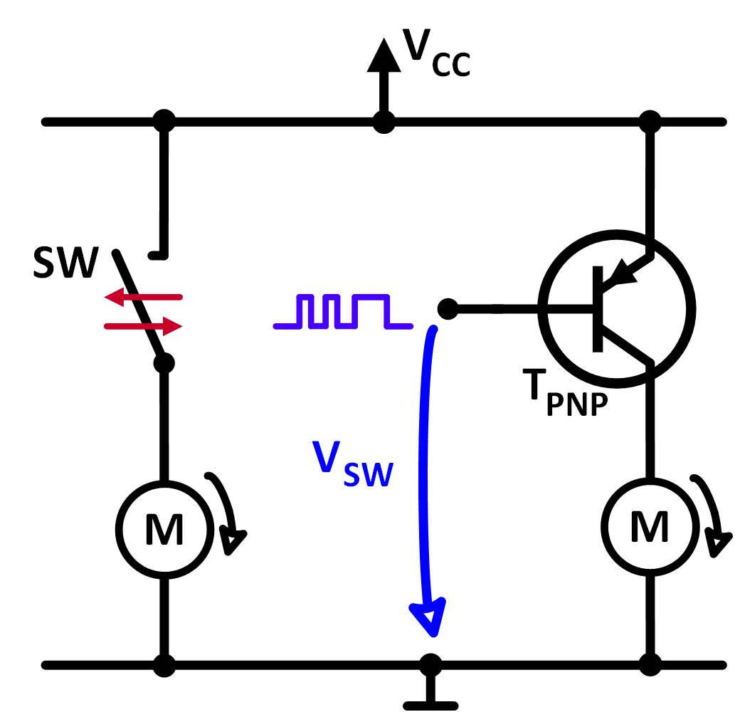
Figure 1: Mechanical switch and pnp transostor as a switch
Korrekte Polarität und Schaltung zur Last
In switch mode, a transistor is operated in a fixed bias configuration. Therefore the load is always connected to the collector
of the transistor. And since the current flows out of the collector of the PNP transistor, the transistor is switched in
current direction in front of the load and not behind the load.
The PNP transistor thus provides a sourcing current and not a sinking current as the NPN transistor would.
Fig. 2 shows the correct and the incorrect installation of the PNP transistor and for comparison the correct wiring of a NPN transistor as a switch.
The PNP transistor thus provides a sourcing current and not a sinking current as the NPN transistor would.
Fig. 2 shows the correct and the incorrect installation of the PNP transistor and for comparison the correct wiring of a NPN transistor as a switch.
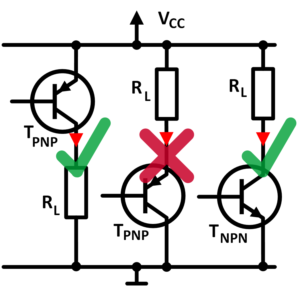
Figure 2: Valid circuits and non wirking circuits of transistors as a switch
Basic circuit of a PNP transistor as switch
In the fixed bias configuration of the PNP transistor as a switch, in addition to the
transistor and the load a base resistor RB is needed.
It defines the base current.
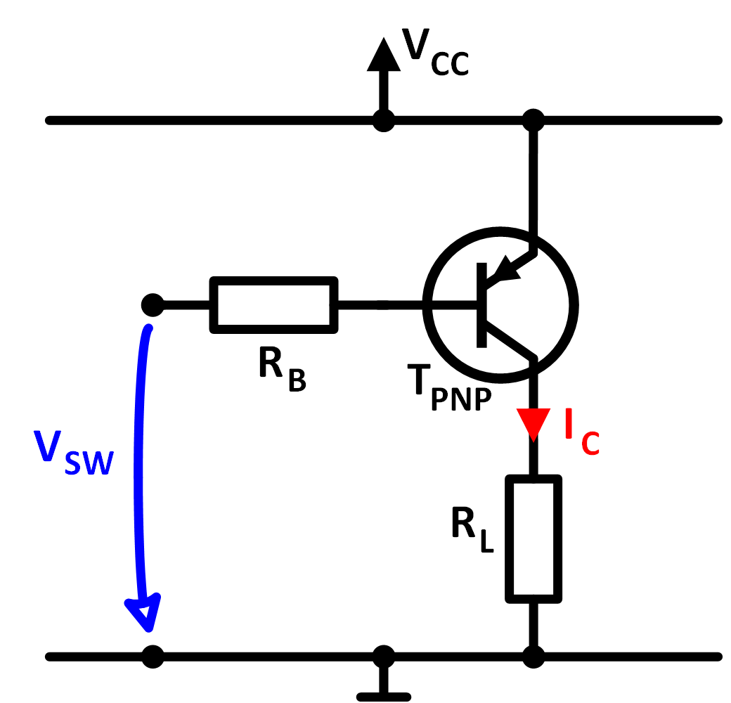
Figure 3: Basic circuit of the pnp transistor as a switch
The base must have the lower voltage potential than the emitter.
The circuit works according to the following simple state table, depending on input V:SW:
| Input VSW | Transistor State |
| VSW = Vcc = High: | Transistor high-Z |
| VSW = GND = Low: | Transistor conducting |
Tabelle 1: State Table PNP Transistor as a switch
Basic circuit with parameters
| Symbol | Parameter |
| RL: | Load resistor |
| RB: | Base reistor |
| VEC: | Emitter- collector- voltage |
| VEB: | Base diode voltage |
| VRB: | Base resistor voltage |
| VSW: | Control voltage |
| Vcc: | Supply voltage |
| GND: | Ground |
| IL: | Load current |
| IB: | Base current |
Tabelle 2: Schaltungsparameter
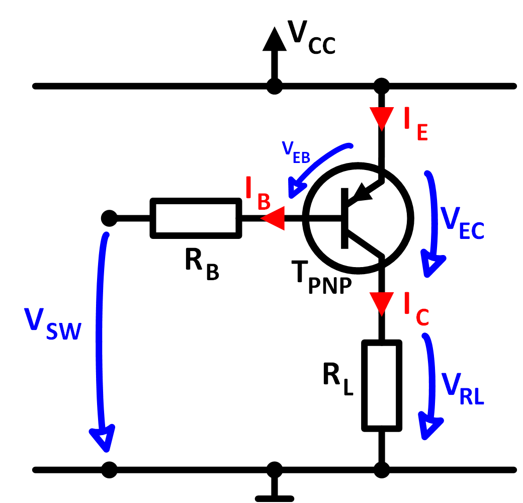
Figure 4: Basic circuit with the designation of all relevant parameters
Calculations
Calculating the component and voltage values is not very difficult. But you need
from the data sheet of the transistor the following parameters:
| Symbol | Parameter |
| VCEsat | Saturation voltage |
| IC max | Max collector current |
| hFE | Current gain factor |
Tabelle 3: Benötigte Parameter aus dem Datenblatt
Calculation of the voltage VRL
First, the voltage VRL is calculated, which drops across RL, when the transistor is conducting.
To do this, subtract the saturation voltage
VECSat, which drops across the transistor, from the supply voltage Vcc.

Figure 5: Formula for calculating the voltage VL across the load
Load current IL
Then the collector current is calculated, which flows through RL when the transistor is switched on.
To do this, divide VRL by the
load resistance RL to get IL.
Can the transistor handle the current?
Now check whether the transistor can withstand the load current. IL must be smaller
than ICmax and IE max from the data sheet.
If the transistor does not withstand the current, a different transistor must be
must be chosen.
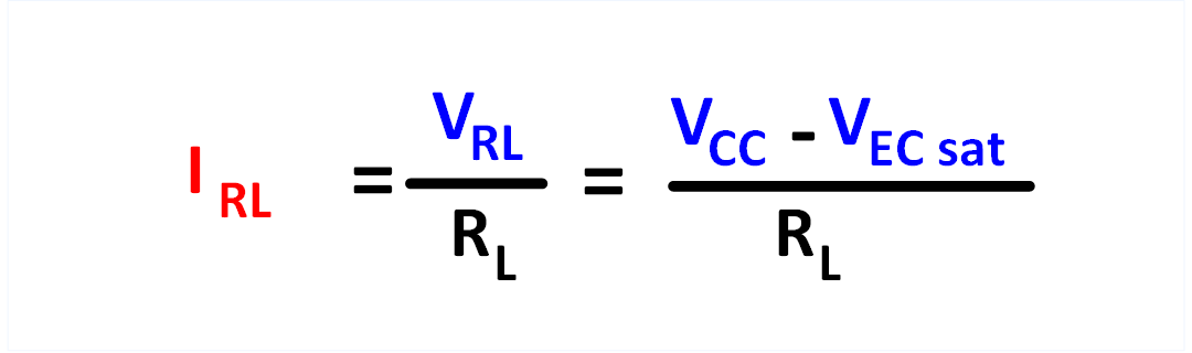
Figure 6: Formula for calculating the load current IL
Base resistor RB
To determine the base resistance RB, first calculate the required
base current IB. Since the transistor in DC mode is a
current amplifier with a fixed amplification factor hFE
a base current is required which is larger than IL divided by hFE.
In order to get make the transistor going into a strong saturation and achieving a
fast switching time, the base current should be 4 to 10 times higher than IFE.
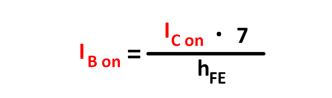
Figure 7: Formula for calculating the base current IB
The voltage across the base resistor of the conduction PNP transistor
is VEB less than the supply voltage Vcc. With this value and
the base current, the required base resistor can be calculated.
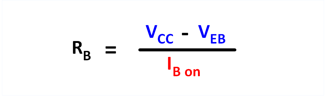
Figure 8: Formula for calculating the base resistor RB
The PNP circuit in the off state
Im sperrenden Zustand wird Vin auf Vcc geschaltet. So kann
kein Strom aus der Basis hinausfliessen, derTransistor sperrt und der Laststrom IL
kommt zum erliegen
In the blocking state, Vin is pulled to Vcc. In this way no current
can flow out of the base, the transistor blocks and the load current IL
gets zero.
Losses in the on state and in the off state
In practice, minimal leakage currents always flow into and out of the transistor in the blocking state.
How large they are can be found in the data sheet of the
transistor data sheet.
And since the transistor remains a low resistance in the conducting state
a small saturation voltage VECsat always remains between emitter and collector.
Despite these losses, the bipolar transistor is a good switch which can be used
for most semiconductor switching applications.
X
Figure 1: Mechanical switch and pnp transostor as a switch
Figure 1: Mechanical switch and pnp transostor as a switch
X
Figure 2: Valid circuits and non wirking circuits of transistors as a switch
Figure 2: Valid circuits and non wirking circuits of transistors as a switch
X
Figure 3: Basic circuit of the pnp transistor as a switch
Figure 3: Basic circuit of the pnp transistor as a switch
X
Figure 4: Basic circuit with the designation of all relevant parameters
Figure 4: Basic circuit with the designation of all relevant parameters
X
Figure 5: Formula for calculating the voltage VL across the load
Figure 5: Formula for calculating the voltage VL across the load
X
Figure 6: Formula for calculating the load current IL
Figure 6: Formula for calculating the load current IL
X
Figure 7: Formula for calculating the base current IB
Figure 7: Formula for calculating the base current IB
X
Figure 8: Formula for calculating the base resistor RB
Figure 8: Formula for calculating the base resistor RB